Overview
Signal polarity mismatches are common at system boundaries. For example, a sensor like the IMD outputs an OK signal, but perhaps the downstream logic would rather capture a FAULT signal - the logical inverse. A single-transistor inverter resolves the mismatch in a small footprint.
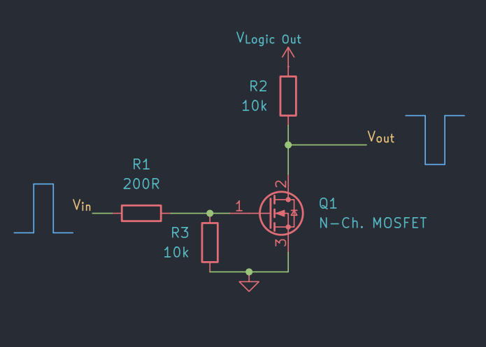
An N-channel MOSFET in a common-source configuration inverts a digital logic signal. When the gate is driven high, the MOSFET turns on and pulls the output low. When the gate is low, the MOSFET is off and a pull-up resistor holds the output high.
This approach suits designs where one or two signals need inverting and an N-channel MOSFET is already in use, which avoids adding unique parts to the BOM. For inverting multiple signals, a dedicated gate IC such as the 74HC04 or 74LVC1G04 is a good, compact option.
Circuit description
The input signal drives the gate of Q1 through series resistor R1. Pull-down resistor R3 holds the gate low when the input is floating or high-impedance. Pull-up resistor R2 connects the drain of Q1 to the supply. The output is taken at the drain, and the source is tied to GND.
- Input high: Q1 saturates, drain pulled to near-GND, output low.
- Input low: Q1 off, drain held at supply through R2, output high.
Design notes
- R1 (gate resistor): Limits current into the capacitive gate during transitions. 100 ohm to 1 kohm is typical for low-frequency logic signals.
- R2 (pull-up resistor): Sets the output high level and the dissipated current when Q1 is on. Lower values reduce rise time but increase static power draw. 4.7 kohm to 10 kohm is typical.
- R3 (gate pull-down): Prevents the gate from floating when the input is disconnected or high-impedance. 10 kohm to 100 kohm is typical.
- MOSFET selection: V_GS(th) must be compatible with the input logic levels. 2N7002 and BSS138 are fully enhanced at 3.3 V and 5 V. Drain current rating is rarely a constraint for signal-level applications.
- Level shifting: There is a built-in opportunity for the inverter to also act as a logic-level shifter. The output swings to the pull-up supply , , not the input signal rail. If is connected to 5V, the output will be 0->5V. If is connected to 3.3V, the output will be 0->3.3V.
Gotchas
Input impedance
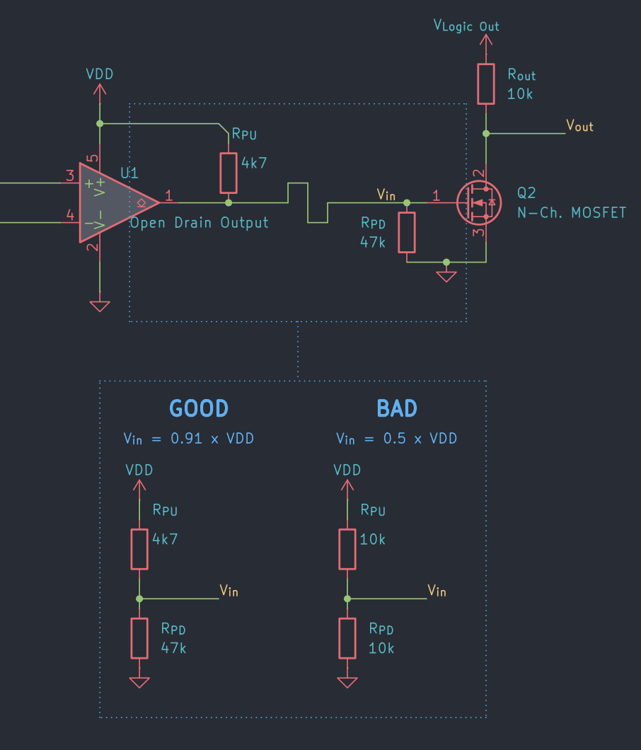
R1 and R3 form a signal path to ground. This is fine for push-pull (low-impedance) sources. If is fed by a higher-impedance source then care must be taken in selecting the resistors involved. For example, an open-drain output with a pull-up resistor is a common logic-signal source, as with the IMD: signal. Here, it is prudent to choose the pulldown to be 3-10x the pullup value. Else, the resulting voltage divider may deny the gate voltage from ever exceeding .
In the schematic below, a comparator U1 with an open drain output drives the inverter. Since U1 is open-drain, a pullup resistor is required. already limits the gate-current, so it does double-duty as the gate resistor. Now there is a current path from VDD to ground through and , which together create a voltage divider and define the maximum gate voltage. If the resistors are equal then the gate voltage will max-out at , which may be too low to properly drive the MOSFET. Setting and means the gate voltage can reach which is likely more acceptable.
Drive is asymmetric
The falling edge is actively pulled low by Q1 (fast), but the rising edge is set by the R2-load RC time constant (slow). For signals above ~400 kHz or into high-capacitance loads, reduce R2 or use a dedicated gate IC.
Meaningful signal names
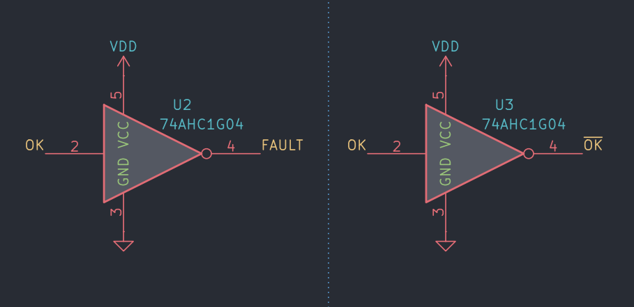
Account for the inversion in your system-level logic. It is easy to lose track of signal polarity when inverters are added mid-design; document active-high vs. active-low conventions at each node by using meaningful net labels: A common convention is to name the signal by what its HIGH state means. For example, an active-high “OK” signal inverts to a “FAULT”, or (“NOT OK”) signal.